Table of Contents >> Show >> Hide
- What Is a Solder Stencil?
- Can You Really Make Solder Stencils With a 3D Printer?
- Why Use a 3D Printer for Solder Stencils?
- FDM vs Resin Printing for PCB Stencils
- Design Workflow: From PCB Paste Layer to Printable Stencil
- Best Print Settings for 3D Printed Solder Stencils
- How to Use a 3D Printed Solder Stencil
- Common Problems and How to Fix Them
- When a 3D Printed Stencil Makes Sense
- Design Tips for Better Results
- Real-World Experiences With Solder Stencils With A 3D Printer
- Conclusion
Note: This article is written for educational electronics prototyping and web publishing. Always follow the safety instructions for your solder paste, printer resin or filament, reflow equipment, and workspace ventilation.
There is a special kind of optimism that appears when a maker looks at a tiny surface-mount PCB and says, “I can assemble that by hand.” Then reality arrives wearing tweezers, holding a 0402 resistor, and laughing quietly. Surface-mount assembly is wonderfully efficient, but applying solder paste pad by pad with a syringe can feel like decorating cupcakes with a fire hose. That is where solder stencils come inand where a 3D printer can become surprisingly useful.
A solder stencil is a thin sheet with openings that match the solder paste pads on a printed circuit board. Spread solder paste across the stencil, lift it away, and the PCB is left with neat paste deposits ready for component placement and reflow. Traditionally, stencils are made from stainless steel, polyimide, or Mylar using laser cutting or chemical etching. Those are still the best options for production work. But for quick prototypes, weekend experiments, school labs, repair jigs, and “I changed one footprint again” revisions, a 3D printed solder stencil can save time, money, and a small amount of sanity.
The idea sounds almost too convenient: export the paste layer from your PCB design, convert it into printable geometry, print a thin stencil, spread paste, and reflow. In practice, the method works best when you understand its limits. A 3D printer is not a magic stencil factory. It is more like a clever assistant that does excellent work when you give it the right job and avoids eye contact when you ask it to print a perfect 0.4 mm pitch QFN stencil on an old wobbly FDM machine.
What Is a Solder Stencil?
A solder stencil, often called a solder paste stencil, is a mask used to deposit solder paste onto PCB pads. It is usually aligned over the board, held flat, and wiped with a squeegee so paste fills the cutouts. When the stencil is lifted, the paste remains on the exposed copper pads. Components are then placed into the paste and heated in a reflow oven, hot plate, skillet, or controlled air system until the solder melts and forms joints.
The key benefit is consistency. Instead of guessing how much paste belongs on every pad, the stencil controls volume by aperture size and stencil thickness. Too much paste can cause solder bridges between pins. Too little paste can create weak joints, tombstoned passives, or open connections. A good stencil makes assembly faster, cleaner, and more repeatable.
Can You Really Make Solder Stencils With a 3D Printer?
Yes, but with a big asterisk wearing safety glasses. You can make useful solder stencils with a 3D printer, especially for larger surface-mount parts, simple boards, and prototype runs. The best results usually come from resin printers because they can produce finer detail and smoother edges than most FDM printers. FDM printers can still work for larger pads, but nozzle diameter, layer height, first-layer squish, and filament stringing make fine apertures difficult.
The practical question is not “Can it be done?” but “What kind of PCB are you trying to assemble?” A stencil for 0805 resistors, SOT-23 transistors, SOIC chips, LEDs, and larger connectors is much more forgiving than a stencil for dense QFNs, BGAs, 0201 passives, or 0.4 mm pitch ICs. If your board looks like it was designed by an ant with an engineering degree, order a professional stencil. If your board has hobby-friendly footprints and you only need a few copies, 3D printing may be worth trying.
Why Use a 3D Printer for Solder Stencils?
Fast Iteration
PCB prototypes change constantly. A footprint gets rotated, a regulator changes package, or a connector moves two millimeters because the enclosure refused to cooperate. Ordering a new stencil for every revision can slow the process. A 3D printed stencil lets you test a board the same day you update the design.
Low Cost for Small Runs
Professional stencils are affordable, but shipping and lead time can still be annoying for one-off builds. If you already own a 3D printer, the material cost for a small stencil can be extremely low. The real cost is tuning time, which is paid in patience and possibly one dramatic sigh.
Integrated Alignment Features
One of the coolest advantages of 3D printing is that the stencil does not have to be only a flat sheet. You can print a frame, board pocket, registration stops, component tray, or hinge features as part of the same design. This turns the stencil into an assembly jig, which can be much easier to use than a floppy sheet taped to a desk.
Useful for Education and Labs
For classrooms, makerspaces, and electronics clubs, printing stencils helps students understand PCB layers, solder paste deposition, aperture size, and reflow workflow. It makes the invisible manufacturing process visibleand occasionally sticky.
FDM vs Resin Printing for PCB Stencils
FDM Printers
FDM printers extrude melted plastic through a nozzle, usually 0.4 mm in diameter. For general 3D printing, that is great. For tiny stencil openings, it is a limitation. The printer must create clean, repeatable holes in a very thin sheet. With a standard 0.4 mm nozzle, apertures smaller than the nozzle width may close up, distort, or become inconsistent.
FDM can be useful for larger components and simple designs. Use a smaller nozzle such as 0.25 mm if available, print slowly, reduce first-layer squish, and choose a material that prints cleanly. PLA can work because it is dimensionally stable and easy to print. PETG is tougher but can string. ABS or ASA may warp. Nylon is probably too flexible for thin stencils unless the design is well supported.
Resin Printers
Resin printers, including SLA, MSLA, and DLP machines, are better suited for detailed stencil work because they can create sharper features and thinner layers. They can print a thin stencil with fine openings more accurately than a typical FDM setup. However, resin printing introduces its own challenges: uncured resin must be cleaned thoroughly, thin prints can warp during curing, and brittle resin may crack if the stencil is flexed too much.
For resin stencils, a tough or flexible engineering resin may be better than a brittle standard resin. The stencil should be washed carefully so apertures are clear, then cured evenly while kept flat. Over-curing can make thin features brittle; under-curing can leave the surface tacky. In other words, resin printing gives better detail, but it still expects you to behave like an adult in the post-processing stage.
Design Workflow: From PCB Paste Layer to Printable Stencil
Step 1: Export the Paste Layer
Start in your PCB design software. In KiCad, Eagle, Altium, EasyEDA, or similar tools, the stencil geometry comes from the paste layer, not the solder mask layer. For a top-side stencil, export the top paste layer. For a bottom-side stencil, export the bottom paste layer separately. Common export formats include Gerber, DXF, SVG, or another vector format that can be converted into a 3D model.
Step 2: Add a Border or Frame
A bare paste layer has only pad apertures. It needs a surrounding body to become a stencil. Add a rectangular frame around the board outline or design a pocket that holds the PCB. Leave enough margin so the stencil can be taped, held, or hinged without flexing into the paste area.
Step 3: Set Stencil Thickness
Commercial prototype stencils commonly fall around 0.1 mm to 0.15 mm thick, though thickness depends on component pitch, paste volume requirements, and assembly process. For 3D printed stencils, thickness is often a compromise between flexibility, print reliability, and paste release. A very thin stencil may print poorly or warp; a thicker stencil may deposit too much paste and cause bridging.
For larger components, a printed thickness around 0.15 mm to 0.25 mm may be workable. For fine-pitch ICs, thickness matters more, and a professional stencil becomes far more attractive. The general goal is simple: deposit enough paste to form reliable joints without creating little solder volcanoes.
Step 4: Adjust Apertures
Stencil openings are rarely just exact copies of copper pads. In professional stencil design, apertures may be reduced, rounded, divided, or modified to control paste volume. For home 3D printed stencils, aperture tuning is even more important because the printer may slightly close small holes or round corners.
For passives, you may reduce apertures slightly to prevent excess paste. For thermal pads under QFNs or power packages, divide the large pad into smaller “windowpane” openings so paste can escape gases during reflow and avoid floating the component. For fine-pitch pins, consider reducing the aperture width if bridging appears. Good stencil design is part engineering, part cooking: too much paste ruins the dish, too little leaves everyone disappointed.
Step 5: Convert to a 3D Model
Depending on your tools, you can convert the exported paste geometry into a DXF or SVG, import it into CAD software, extrude it to the desired thickness, and export an STL or 3MF file. Some workflows use KiCad exports, FreeCAD, OpenSCAD, Fusion, Blender, or slicer tricks to create the model. The exact path matters less than the final result: a flat stencil with clean apertures, correct scale, and reliable alignment.
Best Print Settings for 3D Printed Solder Stencils
For FDM Printing
Use the smallest nozzle you can tune reliably. A 0.25 mm nozzle is much better than a 0.4 mm nozzle for small apertures. Print slowly, keep extrusion calibrated, and use a flat bed surface. Disable aggressive elephant-foot compensation only if it distorts holes; otherwise, use it carefully to prevent first-layer spreading from closing apertures. A single-layer stencil can be tempting, but two or three very thin layers may be more durable depending on your printer.
Consider printing the stencil raised slightly above the bed with support-like geometry or using a very well-tuned first layer. Many failures come from the first layer being smashed too hard, which turns crisp apertures into vague suggestions. If your printer makes strings across openings, dry the filament, lower temperature slightly, improve retraction, and slow travel moves.
For Resin Printing
Print the stencil flat or slightly angled depending on your printer and resin behavior. Flat printing can preserve thickness but may cause suction forces and removal issues. Angled printing can improve peel behavior but may create layer artifacts and require supports. Thin stencils should be washed gently and cured flat between transparent plates or on a flat surface to reduce warping.
Always inspect the apertures after washing. Resin can remain trapped in small holes, especially if the stencil is thick or the openings are narrow. A soft brush, compressed air, or careful rinsing can help clear them. Do not leave uncured resin on a stencil that will contact your PCB or workbench.
How to Use a 3D Printed Solder Stencil
1. Secure the PCB
Place the PCB in a frame, pocket, or border made from spare boards, printed rails, or tape. The board should not slide. The stencil must sit flat against the PCB surface. Any gap allows solder paste to smear under the stencil, which turns precision electronics into abstract art.
2. Align the Apertures
Use corner pads, fiducials, large connectors, or board edges as alignment references. If your printed stencil includes registration walls or pins, test the fit before adding paste. Alignment errors are easier to fix when the board is clean.
3. Apply Solder Paste
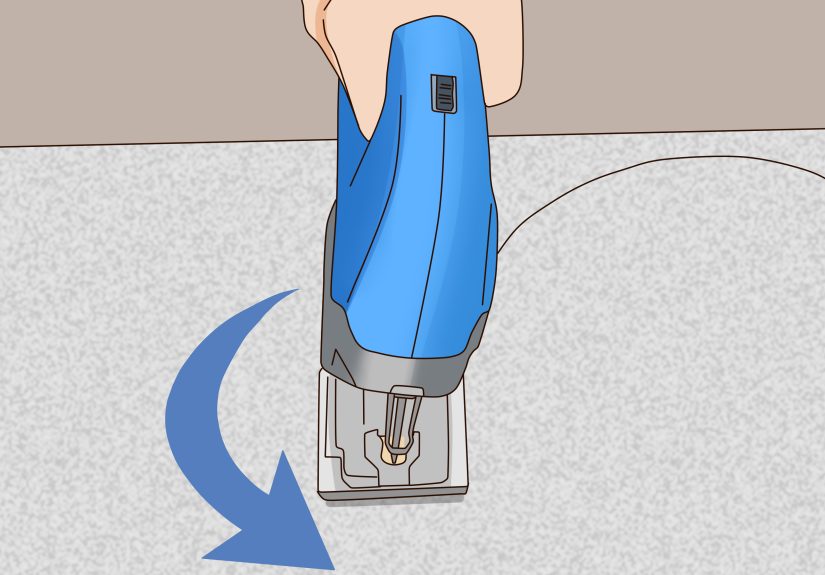
Let refrigerated solder paste warm to room temperature according to the manufacturer’s guidance before use. Stir or knead it only as recommended. Place a small bead of paste at one edge of the stencil and pull it across the apertures with a plastic card, metal squeegee, or printed scraper. Use firm, even pressure. The goal is to fill the openings, not frost a cake.
4. Lift Cleanly
Lift the stencil straight up if possible. A hinge can help keep motion controlled. Check the paste deposits under magnification. If paste is smeared, the stencil may not be flat enough, the paste may be too warm or dry, or the apertures may be rough. If deposits are missing, the openings may be clogged or too small.
5. Place Components and Reflow
Place components carefully with tweezers or a pick-and-place tool. Reflow according to the solder paste profile. Lead-free paste generally requires higher peak temperatures than tin-lead paste. Use proper ventilation because flux fumes can be irritating, and never use food equipment for electronics once it has been used for soldering.
Common Problems and How to Fix Them
Solder Bridges Between Pins
Bridging usually means too much paste, poor alignment, overly large apertures, or a stencil that lifted unevenly. Reduce aperture width for fine-pitch parts, use a thinner stencil, improve alignment, and make sure the stencil sits flush on the board.
Insufficient Solder
If joints look starved or pads are not fully wetted, the stencil may be too thin, apertures may be too small, or paste may not have released cleanly. Clean the stencil, inspect for blocked holes, and slightly enlarge openings where appropriate.
Paste Smearing Under the Stencil
Smearing often comes from poor contact between stencil and PCB. Add a frame the same thickness as the board, tape one side as a hinge, or print a dedicated alignment jig. Also check paste condition; old or badly stored paste can behave unpredictably.
Warped Stencil
Thin printed parts love to warp just when you are feeling proud of yourself. For FDM, improve bed adhesion and cooling consistency. For resin, cure the stencil flat. Store thin stencils between flat sheets when not in use.
Clogged Apertures
Clean the stencil immediately after use. Isopropyl alcohol and lint-free wipes are common for many no-clean pastes, but always check the paste manufacturer’s recommendations. Do not scrape delicate printed apertures with sharp metal tools unless you enjoy redesigning things twice.
When a 3D Printed Stencil Makes Sense
A 3D printed stencil is a strong choice for early prototypes, simple boards, larger SMD parts, educational labs, repair fixtures, and designs that may change frequently. It is especially helpful when the stencil can include alignment features that would be inconvenient with a simple laser-cut sheet.
It is not ideal for production, very fine-pitch components, BGAs, high-density boards, or assemblies where yield matters more than convenience. For those jobs, stainless steel stencils are still the gold standard. They have clean aperture walls, predictable thickness, good durability, and excellent paste release. Polyimide stencils are also popular for prototypes because they are flexible, affordable, and easier to store.
Design Tips for Better Results
First, design for the printer you actually own, not the printer you wish you owned. If your FDM printer struggles with 0.3 mm walls, do not ask it to create a heroic fine-pitch stencil and then act surprised when it produces modern sculpture. Use test coupons before printing the full stencil. Include a few representative footprints from your PCB and compare paste deposits.
Second, add alignment into the model. A stencil that fits around the PCB is easier to use than a loose sheet. Even a simple L-shaped corner guide can improve repeatability. For small boards, a full printed fixture with a shallow pocket can make the process much less fussy.
Third, keep the stencil clean and flat. Solder paste dries, flux residue builds up, and tiny holes clog. Clean immediately after printing paste, inspect under magnification, and store the stencil in a sleeve or between flat panels. A warped stencil is like a bad ruler: technically an object, practically a problem.
Finally, know when to stop tinkering. If you spend six hours tuning a printed stencil to avoid ordering a $10 prototype stencil, the spreadsheet of life may have some questions for you. 3D printing is excellent for speed and learning; professional stencils are excellent for reliability.
Real-World Experiences With Solder Stencils With A 3D Printer
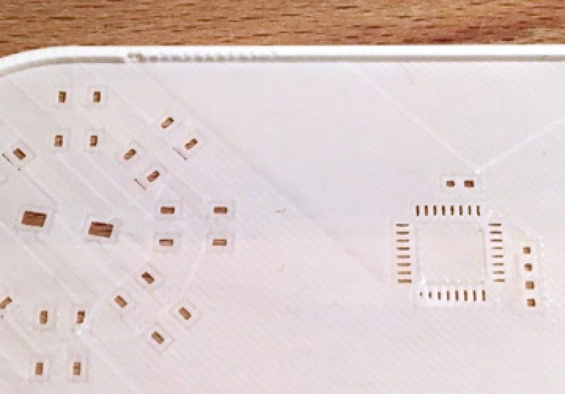
The first experience most people have with a 3D printed solder stencil is not perfection. It is usually a tiny rectangle of plastic that looks promising until you hold it against the light and realize half the apertures are either closed, fuzzy, or shaped like they were cut by a tired squirrel. That is normal. The trick is to treat the first print as a calibration tool, not a final part.
A practical approach is to start with a simple test board. Use common footprints such as 1206, 0805, 0603, SOT-23, SOIC-8, and maybe a 0.65 mm pitch IC. Print only a small stencil section and test paste application. This reveals more than any slicer preview. You will quickly see which apertures release well, which ones bridge, and which ones disappear during printing. After that, you can adjust aperture sizes, stencil thickness, and print settings before risking your actual project.
One useful lesson is that flatness matters as much as resolution. A stencil with beautiful apertures can still perform badly if it bows upward from the PCB. For small boards, a printed pocket works wonders. The PCB drops into the pocket, the stencil surface sits at the right height, and the board cannot slide while you swipe paste. For repeated assembly, adding a taped hinge or printed hinge feature can make the process feel almost professional. Almost. You are still probably using a hotel key card as a squeegee.
Another lesson is that solder paste is not just “gray toothpaste for circuits.” Its condition changes everything. Paste that is too cold may not spread smoothly. Paste that has dried out may roll, skip, or leave ragged deposits. Paste that is too runny can smear under the stencil. Good stencil technique starts before the squeegee touches the board: let the paste reach room temperature, mix only as directed, and use a small amount. More paste on the stencil does not mean better coverage; it usually means more cleanup.
FDM users often discover that the first layer is both friend and enemy. A nicely squished first layer helps adhesion, but it can also shrink aperture openings. If your holes are closing, reduce first-layer flow, increase elephant-foot compensation, raise the Z offset slightly, or print on a smoother surface. A smaller nozzle helps, but only if the printer is calibrated. A poorly tuned 0.25 mm nozzle can be worse than a well-tuned 0.4 mm nozzle for simple footprints.
Resin users usually get better detail but face cleaning and warping challenges. Thin resin stencils can curl after curing, especially if one side receives more UV exposure than the other. Curing between flat transparent plates can help. So can designing a thicker outer frame with a thinner aperture region. Resin also needs careful washing because uncured resin trapped in apertures will ruin paste release. A stencil that looks clean at arm’s length may still have blocked holes under magnification.
The most satisfying moment comes after reflow. When the parts pull into alignment and the solder joints shine evenly, the whole process feels slightly magical. The stencil, the paste, the component placement, and surface tension all cooperate for a few seconds. But the best makers still inspect every board. Look for bridges, tombstoned parts, shifted ICs, dull joints, and unsoldered pins. A 3D printed stencil can make assembly faster, but it does not eliminate inspection.
For many hobbyists, the winning setup is hybrid: print stencils and jigs for early revisions, then order a professional stencil once the PCB design stabilizes. That gives you the speed of desktop fabrication without pretending it can replace industrial tooling in every case. In other words, use the 3D printer as a rapid prototyping tool, not as a tiny factory with delusions of grandeur.
Conclusion
Making solder stencils with a 3D printer is one of those maker techniques that sits perfectly between clever and slightly ridiculousin the best possible way. It will not replace stainless steel stencils for serious production, fine-pitch assembly, or high-yield manufacturing. But for prototypes, simple SMD boards, educational projects, and fast design iterations, it can be genuinely useful.
The secret is understanding the whole workflow: export the paste layer, design a flat and well-aligned stencil, choose the right printing process, tune the aperture geometry, apply paste carefully, and inspect the results. FDM printing can work for larger footprints when tuned well. Resin printing offers better detail but needs careful post-processing. Either way, success depends less on luck and more on testing, measurement, and not blaming the PCB when the stencil was obviously warped.
If you build electronics regularly, a 3D printed solder stencil is worth adding to your toolkit. It is cheap, fast, customizable, and surprisingly educational. It also gives your 3D printer a break from making benchy boats, cable clips, and mysterious brackets labeled “final_final_v7.stl.”